
How to Fix Discord Error: 'Installation Has Failed'
🕤 11 Jan 2025 Read more

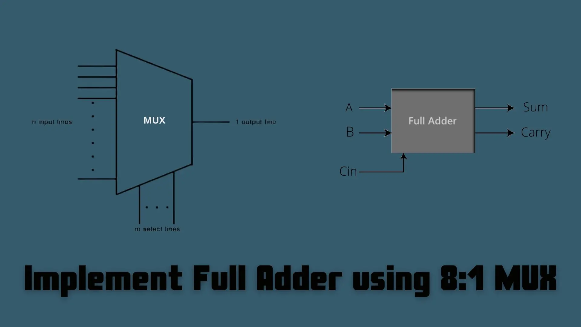
Multiplexers and Adders is one of the important circuits in Electronics.
A multiplexer is a combinational circuit with many data inputs and based on control inputs, single data outputs are generated.
For N:1 MUX, N number of input lines is required, and log2n number of control/selection lines is required.
We can implement various circuits using MUX, to reduce no. of wires, and reduce circuit complexity and cost.
A full adder is a combinational logic circuit that can add two binary digits plus a carry-in digit to produce a sum and a carry-out digit. There total 3 inputs are required and 2 outputs are generated (sum and carry)
Full Adder is used to perform operations like addition or subtractions. Full Adder is used in the ALU and other processor parts to generate memory addresses, and table indices, set the program counter to the next instruction, and many other functions.
Sometimes we will not get Full Adder in the Market and we have to design Full Adder using another Circuit. The multiplexer is one of the circuits for creating a Full Adder.
Let's design Full Adder using 8:1 MUX
First, let's look at the truth table of Full Adder:
| A | B | Cin | S | Co |
| 0 | 0 | 0 | 0 | 0 |
| 0 | 0 | 1 | 1 | 0 |
| 0 | 1 | 0 | 1 | 0 |
| 0 | 1 | 1 | 0 | 1 |
| 1 | 0 | 0 | 1 | 0 |
| 1 | 0 | 1 | 0 | 1 |
| 1 | 1 | 0 | 0 | 1 |
| 1 | 1 | 1 | 1 | 1 |
Here we can clearly notice only 4 outputs, Sum(S) = 1 and are listed below
| A | B | S |
| 0 | 0 | 1 = Io = Cin |
| 0 | 1 | 1 = I1 = Cin' |
| 1 | 0 | 1 = I2 = Cin' |
| 1 | 1 | 1 = I3 = Cin |
Also, Here we can clearly notice only for 4 outputs, Carry(Co) = 1, and are listed below.
| A | B | Carry |
| 0 | 0 | 0 |
| 0 | 1 | Cin |
| 1 | 0 | Cin |
| 1 | 1 | 1 |
As a result, we have implemented Full Adder using only 1 MUX and do not need two XOR gates, as we did when we made Full Adder using Basic Logic Gates.
Let's look advantages of using an 8:1 multiplexer to implement a full adder:
Let's look disadvantages of using an 8:1 multiplexer to implement a full adder:


.png)