-(1).jpg)

Mobile Mastery: Transforming Work Habits with 8 iOS Productivity Techniques
🕤 07 Jan 2024 Read more

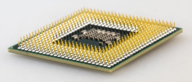
When you go to the market to buy a laptop or a phone, the retailers will explain the various features of those electronic devices to you. They may have told you that it has a 7nm CPU size or a 10nm processor size. You may have heard this from them. This is an outstanding processor; it consumes less power, consumes less heat, the battery lasts longer, the processing speed is greater, etc. Then there are some thoughts running through your head, such as Uff what the hack is "nm." This article will help you understand what nm means in a processor.
nm stands for Nanometer. nm is a unit of measurement for length in a metrics system just like meters, centimeters,s, etc. It is used to express dimensions on the atomic scale. In technical terms, it is referred to as a "process node" and "technology node". You will be clear with the following metrics comparison if you cannot compare or obtain the value.
So,
1nm = 0.00000001 cm = one billionth of a meter.
Therefore, 1nm is very very small which we cannot measure in daily life. It is used in the company which uses nanometer technology for measuring smaller items like measuring the distance between adjacent transistors in processor design, and the size of the transistors used in our phones, laptops, tablets, etc.
Many chipset manufacturing companies like TSMC, Samsung, Intel, etc. use nanometers as units in manufacturing processes. It tells how packed transistors are present inside the processor.
The number of transistors used in electronic devices differs according to their use.
CPUs are made up of billions of transistors and are housed in a single chip. The smaller the distance between transistors in the processor (in nm), the more transistors can fit in a given space. As a result, the distance traveled by electrons to perform useful work is reduced. This ultimately results in faster computing power, less energy consumption and heat dissipation, less thermal output around the board, and a smaller die size, which ultimately reduces costs and increases transistor density of the same size, resulting in more cores per chip. Intel currently employs 10nm or 14nm technology, while TSMC employs 7nm technology. These are the processor's lithography.
Normally speaking, TSMC 7nm processor has a more compact no. of the transistor in a given space, so, they dissipate less heat, consume less power, faster computing power than TSMC 14nm processor. This is only just one factor in determining better phones and laptops. There are also other factors like the amount of RAM, graphics unit, HDD, etc.
There are various benefits of having a lower nm lithography CPU some of them explain pointwise :
1 Faster Transistor: The distance between the source and drain of a transistor will be smaller in a lower nm processor and the distance between the transistor decreases so the electricity or we can say the electron has to travel less distance for doing the task.
2 Lower Power Transistors: In lower nm CPUs, transistors can switch the state(on/off) with less power. The lower nm process will be more electrically efficient. In the case of a CPU with fewer nanometers, the switching of the transistors requires a modest amount of power.
3 Higher Transistor Density: Having smaller transistor sizes and distances between the transistor you can fit more transistors in a given area. Take a two-processor with the same die size and let's say one uses a smaller value manufacturing process than the other and one with a smaller manufacturing process will fit more transistors in it.
4 Less Heat Dissipate: When the electronic device consumes less power then automatically CPU will generate less heat.
5 Less Cooling Required: As the heat dissipation is low, less cooling and cooler may be required.
6 More Space per chip and more cores per CPU
The main significance of nm in the processor is a measure of the size of transistors that are used to make up the processor. If the size of transistors is small then more transistors can be adjusted into a given space which can improve the performance and power efficiency of the processor.
The underlying problem with silicon transistors is that, at 7 nm, the transistors sit so near to each other that, if the processor manufacturer company try to shrink them any more to 5 nm or 3 nm, a process known as quantum tunneling will enter the picture. This creates a fundamental problem for the technology. Because of this impact, it is, unfortunately, the case that the transistor cannot be reliably shut off and will, for the most part, continue to remain on.
Therefore, the physical constraints of silicon are extremely real, and they in reality generate significant difficulties when working with it. Because of this, it is necessary to keep a constant eye on the production process as well as the process curve. Therefore, each of the factors, as well as their behavior, needs to be carefully tracked. This has proven to be a significant obstacle for foundries.
Adoption of new technology: The process of patterning that is used for today's chips is called photolithography, and it operates using a light source that has a wavelength of 193 nm. However, a new technology known as EUV lithography is now under development, and it operates using a light source that has a wavelength of 13.5 nm. This newly developed processing technology and set of procedures present processor designers with a fresh set of hurdles. It is said that EUV helps enable advanced chip scaling.
If you want in pointwise then here are some of them:
Moore's Law is just an observation or predictable analysis given by Gordon Moore in 1965 that the number of transistors used in a silicon chip doubles every two years. So, we can expect the capability and speed of our electronic devices to increase every couple of years.
According to another perception of Moore's law, the development of a microprocessor is exponential. This seems to nearly follow as shown below.
Today smartphones, laptops, game consoles,s or any electronic devices would not be possible if this development has not occurred.
Now, let's talk about 14nm, 10nm, 7nm, and other nm technology.
This nm are nanometer values and note that there is no universal standard to calculate nanometer value. Different processor manufacturer calculates it in a different way. So, 10nm TSMC is not equivalent to 10nm Intel and 10nm Samsung.
As they differ from company to company, these days nm in the processor are just becoming like marketing numbers.

So note that we are comparing these nm technologies on the basis of one processor manufacturing company let's say: Intel
Currently, intel does not have a 7nm processor size. It is said that by 2023, Intel 7nm processor will arrive.
The lithographic process of 5 nanometers (5 nm) is a semiconductor process for the production of nodes after the 7 nm process node. Its manufacturing process begins around 2020. There is no Intel processor having a 5nm process. The first 5-nanometer process technology features FinFET-Transistors with nanometers with fin pitches in the 20s of nm and densest metal pitches in the 30s of nm.
The lithographic process of 3 nanometers (3 nm) is a semiconductor process for the production of nodes after the 5 nm process node. Its commercial mass production will begin around 2023.
IBM recently announced the world's first 2nm process. According to them, they provide 45% high performance and 75% lower energy use than modern 7nm process design.
The current nm process uses electrons through silicon paths in the transistor for moving information. The next evolution of the chip can be photonics which inside of electrons traveling on silicon paths tiny packets of light (photons) will travel and increase in speed with less power consumption. Scientists are working on this. Hope this is the future.
FAQ:
Ans: There are lots of R & D going on. A team at Lawrence Berkeley National Laboratory has created a functional 1-nanometer-long transistor gate, which the lab claims is the smallest working transistor ever created. They claim that by switching from silicon to MoS2, we can create a transistor with a gate as short as 1 nanometer and use it as a switch. (source).
There is currently no 1nm Processor. Making a 1nm process for R&D may be possible, but making a fully functional processor is not. Making a very small nm process will require dealing with issues such as quantum effects, which are extremely difficult to handle.
Ans: Every possible thing is not viable. 1nm processors may be more expensive than 7nm and 10nm processors. Furthermore, tolerance to minor defects for 1nm processors may be lower than for 7nm and 10nm processors. Extensive R&D research may also be required to reduce costs and tolerance.
Ans: Building a smaller transistor will require a much more expensive factory and R & D costs etc.
Ans: We can't go below 1 nm because then you'd have to figure out how to make a transistor out of half an atom, which the world is not able to do till now.
In order to construct an integrated circuit, lithography is the procedure that involves employing sensitized layers to print the integrated circuit and its components. After that, the sensitized layer is etched chemically to eliminate any undesirable material, which is typically composed of copper and silicon compounds, leaving the circuit in its place.
Reference:
3) wikipedia
4) Lithography


.png)


.jpg)